Realistic opamp
UNDER CONSTRUCTION
Contents
- Introduction
- Prepare a simple circuit
- Concept check
- Realistic opamp model and default parameters
- MNA References
Introduction
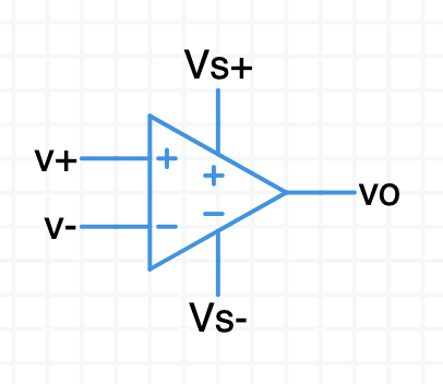
This opamp model is a differential amplifier with semi-realistic properties. It measures the difference in voltage between its two input ports. It amplifies that difference by the gain factor $\text A$ (default: $100{,}000$) and puts the result on the output port.
$\sf{vo} = \text A (\sf v$+ $- \,\,\sf v$-$)$
This realistic opamp model has two power supply pins, $\small{\sf{Vs+}}$ and $\small{\sf{Vs-}}$. The power supplies limit how far the output voltage, $\sf{vo}$, can swing. $\sf{vo}$ is always be between the two supply voltages.
The model has a high input resistance between the input pins (default: $1\,\text M \Omega$), and a small output resistance in series with the output driver (default: $1\,\Omega$). Both of these parameters, and the gain, can be adjusted by double-clicking on the opamp symbol.
For more details see the Circuit Sandbox opamp model.
Prepare a simple circuit
Open this incomplete realistic opamp schematic.
Double-click on the opamp. Give it a name like “Op1”.
The gain of this opamp has been set low so you can see how a differential amplifier works. What is the gain?
show answer
The initial gain setting is $\text A = 10$.
Opamps have gains in the many $1000$’s, but we start low to get a feel for how it works.
Add another opamp from the parts bin. Open up its properties with a double-click.
What is the gain of an opamp fresh from the parts bin?
What is the input resistance?
What is the output resistance?
show answer
A default opamp in Circuit Sandbox has a gain of $\text A = 100{,}000$.
The input resistance is $1\,\text M\Omega$. (The resistance between $\sf v$+ and $\sf v$-.)
The output resistance is $1\,\Omega$. (Resistance in series with the output pin.)
You can leave these values alone most of the time.
We don’t need this opamp any more. Please delete it from your schematic.
Build a circuit,
- Power: This opamp model requires two power inputs. Representative power supplies are provided. Connect power to the opamp,
- Double click each voltage source and set the voltage of both to $12\,\text V$. A typical opamp supply is between $5$ an $15$ volts.
- Move the two ???— labels so they connect to the opamp. Double click to change their names to $\sf Vs+$ and $\sf Vs-$. This makes the connection to the power supply.
- Alternatively, delete the node labels and wire the supplies directly to the opamp.
- Add a ground symbol to the node between the two sources. (Select the ground symbol and rotate it by tapping R on the keyboard.)
- Inputs: Connect the two input voltage sources,
- $\sf v$+ to the opamp’s + input
- $\sf v$- to the opamp’s - input
- Add a ground symbol to the bottom of each input source.
- Add a probe,
- Move the voltage probe so it touches $\sf{vo}$.
finished schematic
Do the rest of this exercise with your own schematic.
If you want you can compare it to the one I drew — Willy’ schematic.
Concept check
With the inputs as given, figure out in your head what $\sf vo$ will be.
Hint: Fill in the opamp equation, $\sf{vo} = \text A \,[(\sf{v+}) - (\sf{v-})]$.
Perform a DC operating point analysis (click on DC).
What is $\sf vo$? Did you guess right?
show answer
$\sf{vo} = \text A \,[(\sf{v+}) - (\sf{v-})]$
$\sf vo = 10 \,(1.1 - 1)$
$\sf vo = 10 \,(0.1)$
$\sf vo = 1\,\text V$
It actually comes out $0.98\,\text V$. I don’t know why, yet. The gain appears to be 9.8 instead of 10.
The output voltage is $10$ times the difference between $\sf v$+ and $\sf v$-.
Change $\sf v$+ to $3\,\text V$. What is going to happen to $\sf vo$?
Anticipate the answer in your head. Then perform a DC simulation.
show answer
The expected answer is $(3 - 1)\times 10 = 20\,\text V$. But the result is actually close to $12\,\text V$. Why is that?
That’s because the output cannot exceed the power supply. The opamp is saturated.
Change $\sf v$+ to $-3\,\text V$. What will happen to the output?
Anticipate the answer in your head. Then perform a DC simulation.
Voltage transfer plot
Change $\sf v$- to $0\,\text V$.
Change $\sf v$+ to a triangle wave with these parameters,
- Initial value: $-4$
- Plateau value: $+4$
- Frequency (Hz): $0.5$
Add a second voltage probe to $\sf v$+. Change it’s color to something different than the other probe.
Click on TRAN and run a transient simulation for 1 second. This is an approximation to a voltage transfer plot. Sweeping the input voltage from $-20$ to $+20$ shows you the output voltage starts in negative saturation at the negative power rail, then becomes linear with a slope of GAIN, and finally saturates at the positive rail.
Special probe setting: Select the $\sf v$+ probe you added. Change its color to “x-axis”. Perform the same TRAN again.
Notice the input probe now appears as the x-axis of the plot. This is a proper voltage transfer plot, $v_{out}$ vs. $v_{in}$.
Voltage transfer circuit model
Under construction.
Realistic opamp model and default parameters
Input resistance $R_{in} = 1\,\text M\Omega = 10^{+6}$, resistance between input terminals.
Output resistance $R_o = 1\,\Omega$, resistance in series with output driver.
Amplification $A = 100{,}000 = 10^{+5}$
$G_{in} = 1/R_{in}$
$G_o = 1/R_o$
$G_{leak} = \dfrac{G_{in}}{(1 + A)} = 10^{-11} \quad (10^{11}\Omega)$, leakage power supply to inputs.
$G_{int} = \dfrac{G_o}{(1 + A)} = 10^{-5} \quad (100\,k\Omega)$, determines slew rate
$G_{thru} = \dfrac{G_o}{100} = 0.001 \quad (100\,\Omega)$, models power consumption.
$I_{max} = G_{int} \times 10^6 = 10 \quad$ sets the slew rate to $10\,v/\mu s$
Open-loop $3\,\text{dB}$ point is $\text{TBD Hz}$
Another stab at the opamp model.
MNA References
Joe Steinmeyer — Professor Jacob White was one of the folks who wrote the book on numerical simulations for circuits in the 80’s and 90’s so I’m sure there’s some genius stuff going on. If I’m looking at the right part it just looks like a current source driving a resistor with a gain based off of the gain (so he’s summing some internal feedback)… Then whatever the output ends up being he assigns that to the appropriate supply.
https://www.analog-electronics.eu/-electronics/modified-nodal-analysis/modified-nodal-analysis.xhtml
https://ieeexplore.ieee.org/document/1015781 L. M. Wedepohl and L. Jackson, “Modified nodal analysis: an essential addition to electrical circuit theory and analysis,” Engineering Science and Education Journal, vol. 11, pp. 84–92, June 1992.
https://ieeexplore.ieee.org/document/662284 A formulation method for including ideal operational amplifiers in modified nodal analysis
https://ieeexplore.ieee.org/document/4321725 Development of Modified Nodal Analysis into a Pedagogical Tool
https://onlinelibrary.wiley.com/doi/pdf/10.1002/9781119078388.app2 Modified Nodal Analysis Stamps
Original MNA paper:
C. Ho, A. Ruehli, and P. Brennan. The modified nodal approach to network analysis. IEEE Transactions on Circuits and Systems, 22(6):504–509, June 1975. pdf
Swarthmore:
Introduction to Circuit Analysis with Matlab: https://lpsa.swarthmore.edu/Systems/Electrical/mna/MNA1.html (revised version)
Opamps: https://lpsa.swarthmore.edu/Systems/Electrical/mna/MNA5.html.
“The equation for the op-amp is not in terms of the voltage at its output, but rather it specifies that the two input terminals are at the same potential.”
“Caveat: The two ideal op-amp assumptions (no input current, no potential difference at inputs) only hold for circuits with negative feedback. Because of this, the MNA method as applied here can give erroneous results if negative feedback is not present. This problem actually persists in many commercial circuit simulators – you can hook up a circuit with the input terminals reversed (so that it would not operate properly in practice due to lack of negative feedback) and the simulation behaves as if there is no problem. Note also that the output of the op-amp is not limited by any power supply – this circuit will happily generate hundreds of volts.”
Referenced by Circuit Sandbox’s simulation engine,
https://www.analog-electronics.eu/analog-electronics/modified-nodal-analysis/modified-nodal-analysis.xhtml. This link may come alive in the future. In the meantime, here’s a copy of the article, MNA